Adapting Operational Volume Scanning to Low-Power FMCW: System Development and Physically-Informed ML Calibration
Asif Awaludin,
Dwiyanto,
Rahmat Triyono,
Yunus Subagyo Swarinoto,
Erwin Makmur,
Beno Kunto Pradekso,
Oktanto Dedi Winarko,
Muhammad Farras Archi Maggaukang,
Liarto,
Donaldi Sukma Permana,
Roni Kurniawan,
Rezky Yunita,
Mohamad Husein Nurrahmat,
Thahir Daniel Foreigner Hutapea,
Agung Majid,
Muhamad Rifki Taufik,
Warjono,
Ferdinandus Edwin Penalun,
Bobby Harnawan,
Dodi Dian Patriadi,
Muhammad Rendi Anggara,
Hastuadi Harsa,
Alfan Sukmana Praja,
Fatkhuroyan,
Wido Hanggoro,
Muhammad Najib Habibie,
Welly Fitria,
Rahayu Sapta Sri Sudewi,
Asteria Satyaning Handayani,
Sri Noviati and
Vestiana Aza
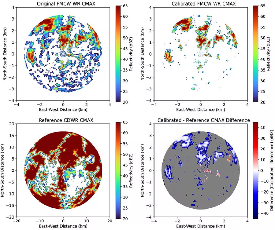
This study presents the development and evaluation of a transportable X-band frequency-modulated continuous-wave (FMCW) weather radar (WR) that successfully adapts operational volumetric scanning strategies typically reserved for high-power to low-power pulsed systems. The radar integrates a complete radio-frequency chain, a carbon graphite antenna, and a dedicated real-time processing unit designed for operational volumetric scanning. It performs rapid 4-minute volume scans across seven elevation angles (0.00˚-15.88˚) with non-uniform spacing optimized for low-level atmospheric sampling, while a 2 RPM rotation provides full azimuthal coverage every 30 s. The resulting Column Maximum (CMAX) product synthesizes reflectivity from all elevation angles to depict three-dimensional precipitation structure, demonstrating a spatial observational capability distinct from traditional profiling FMCW radars. A three-stage hierarchical physically-informed architecture calibration framework was implemented to ensure quantitative accuracy in the FMCW WRs measurements, using collocated C-band Doppler Weather Radar (CDWR) observations as reference data. Validation through internal five-fold Group K-Fold cross-validation, Leave-One-Pair-Out (LOPO) testing, and external evaluation using independent radar pairs demonstrated the frameworks robustness. The case study of localized urban convection observed by the FMCW WR shows that the developed low-cost radar offers much finer range resolution and can reveal detailed structures within convective cells.